What is EMI / RFI Shielding? Essential Guide to Protecting Your Devices.
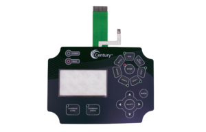
Shielding, in the context of Membrane Keypads and keyboards, refers to the use of materials and techniques to protect electronic components from Electromagnetic Interference (EMI) and radiofrequency interference (RFI). EMI and RFI are forms of electromagnetic pollution that can potentially disrupt the proper functioning of electronic devices by introducing unwanted electromagnetic signals. In the case of Membrane Keypads and keyboards, shielding is employed to minimize the impact of such interference and maintain the reliability and performance of the input device.
The materials and inks used for shielding in HMI Input Devices typically fall into the following categories:
1. Conductive Inks:
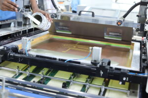
- Silver Ink: Silver-based conductive inks are commonly used in Membrane Keypads and keyboards for creating conductive traces. These inks provide good conductivity and can be applied in various printing methods, including screen printing and inkjet printing.

- Carbon Ink: Carbon-based inks are another option for creating conductive elements in Membrane Keypads. They are cost-effective and can be applied using screen printing methods.
- Copper Inks: Copper-based conductive inks are used in some applications, offering good electrical conductivity.
2. Shielding Materials:
- Transparent Shielding Films: Transparent films with conductive properties, such as metalized polyester films, can be applied to display surfaces. These films offer EMI shielding while maintaining optical clarity.
- Conductive Films: Thin conductive films, often made of materials like copper or aluminium, can be used to provide shielding. These films are typically applied to the Membrane or the PCB (Printed Circuit Board) layers of the keypad.
- Metal Foils: Thin metal foils, such as copper or aluminium foils, can be used as shielding materials. These foils are applied to the keypad or keyboard components to create a conductive barrier against Electromagnetic Interference.
- Conductive Fabrics: Some Membrane Keypads may incorporate fabrics with conductive properties for shielding. These fabrics can be integrated into the keypad structure to provide a flexible and conductive shield.

3. EMI / RFI Shielding Coatings:
- Conductive Coatings: Specialized coatings with conductive properties can be applied to the surface of the keypad or keyboard components. These coatings form a protective layer that shields against EMI and RFI.
- Transparent Conductive Coatings: In touchscreens and display applications, transparent conductive coatings made of materials like indium tin oxide (ITO) or silver nanowires may be used to maintain optical clarity while providing shielding.
- Metalized Coatings: Coatings containing metal particles or flakes, such as nickel or silver, can be applied to provide shielding. These coatings are designed to create a conductive surface that helps in dissipating Electromagnetic Interference.
What are the different types of patterns used in shielding?
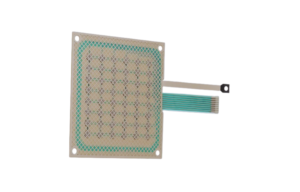
Shielding patterns refer to the configurations or designs of conductive elements used to protect electronic components from Electromagnetic Interference (EMI) and Radiofrequency Interference (RFI). These patterns are often applied using conductive materials, such as metals or conductive inks, to create a barrier against unwanted electromagnetic signals. Here are some common shielding patterns:
Grid Pattern:
-
- Description: A grid of intersecting horizontal and vertical conductive lines or traces.
- Application: Used in various electronic devices, including touchscreens, displays, and printed circuit boards (PCBs).

Mesh Pattern:
-
- Description: A mesh-like structure of interconnected conductive lines.
- Application: Commonly used in Electromagnetic Interference (EMI) layer materials and screens, such as mesh windows on electronic enclosures.
Crosshatch Pattern:
-
- Description: A pattern of diagonal lines that form a crosshatch or lattice.
- Application: Employed in electronic components and circuits to minimize interference.
Spiral Pattern:
-
- Description: A continuous spiral of conductive material.
- Application: Used in applications where a continuous, winding pattern is more suitable, such as antennas or inductors.
Finger stock Pattern:
-
- Description: Finger-like projections of conductive material arranged in a pattern.
- Application: Commonly used in EMI gaskets and seals for enclosures to ensure a continuous conductive contact.
Random Pattern:
-
- Description: A non-repetitive arrangement of conductive elements.
- Application: Applied in situations where a uniform and predictable pattern may not be necessary or feasible.
Diamond Pattern:
-
- Description: Conductive shielding lines arranged in a diamond-shaped grid.
- Application: Used in EMI shielding for various electronic devices.
Island Pattern:
-
- Description: Discrete islands or patches of conductive material.
- Application: Applied in situations where specific areas need shielding, leaving other areas open.
Waffle Pattern:
-
- Description: A grid pattern with each cell resembling a waffle or honeycomb structure.
- Application: Used in some EMI shielding applications for its geometric arrangement.
Conductive Coating Pattern:
-
- Description: A conductive coating applied uniformly over a surface.
- Application: Used in coating electronic components or surfaces to provide a conductive shield.
The Protolab expert team selects a shielding Ink, Pattern, and Material based on considerations such as the device application, interference characteristics, and manufacturing constraints. The team aims to design an effective and continuous conductive barrier that attenuates Electromagnetic Interference, aligning with the specific requirements of the application. This strategic approach ensures optimal performance, preventing unwanted signals from impacting the functionality of electronic components.


I appreciate you sharing this blog post. Thanks Again. Cool.
Attractive section of content I just stumbled upon your blog and in accession capital to assert that I get actually enjoyed account your blog posts Anyway I will be subscribing to your augment and even I achievement you access consistently fast
Wow, what a fantastic blog style. How long have you been blogging for? You made it seem so simple. Your website looks beautiful overall, and the information is even better.
I do agree with all the ideas you have introduced on your post They are very convincing and will definitely work Still the posts are very short for newbies May just you please prolong them a little from subsequent time Thank you for the post
Simply wish to say your article is as amazing The clearness in your post is just nice and i could assume youre an expert on this subject Well with your permission let me to grab your feed to keep updated with forthcoming post Thanks a million and please carry on the gratifying work
Wonderful web site Lots of useful info here Im sending it to a few friends ans additionally sharing in delicious And obviously thanks to your effort
hiI like your writing so much share we be in contact more approximately your article on AOL I need a specialist in this area to resolve my problem Maybe that is you Looking ahead to see you
Wonderful insight on the Conductive ink usage. Are you a conductive ink manufacturer as well?
you’re really a good webmaster. The web site loading speed is incredible. It seems that you are doing any unique trick. Furthermore, The contents are masterpiece. you have done a wonderful job on this topic!
Simply wish to say your article is as amazing The clearness in your post is just nice and i could assume youre an expert on this subject Well with your permission let me to grab your feed to keep updated with forthcoming post Thanks a million and please carry on the gratifying work
It’s really a cool and helpful piece of info. I’m happy that you simply shared this helpful information with us. Please stay us up to date like this. Thank you for sharing.
Magnificent beat I would like to apprentice while you amend your site how can i subscribe for a blog web site The account helped me a acceptable deal I had been a little bit acquainted of this your broadcast offered bright clear idea
I was recommended this website by my cousin I am not sure whether this post is written by him as nobody else know such detailed about my difficulty You are wonderful Thanks
Nice blog here Also your site loads up very fast What host are you using Can I get your affiliate link to your host I wish my site loaded up as quickly as yours lol
Gracias por la informacion. Saludos. Gracias!
Gracias por tu aportacion. Saludos. Un cordial saludo!
I just wanted to take a moment to say how much I appreciate your blog posts. They’re always well-written, informative, and keep me coming back for more. Keep up the great work!
I do not even know how I ended up here but I thought this post was great I dont know who you are but definitely youre going to a famous blogger if you arent already Cheers
Wow! Thank you! I continually wanted to write on my website something like that. Can I take a part of your post to my website?
Muy buen post. Saludos. Gracias!
Impressive write-up
Well structured